If you are looking for Two Layer Pcb, you are in the right place. We have 34 images of Two Layer Pcb, including pictures, photos, wallpapers, and more. On this page, we also have a variety of images available, such as png, jpg, animated gifs, artwork, logos, black and white, transparent, and more.
Not only Two Layer Pcb, but you can also find other images such as Most Complex, RF Resistor, Design, Schematics, Holding Pins, Printed, Layout Design, Board Design, Circuit Board, Circuit Board Components, Prototype Board, Assembly Line, Normal PC, Full Form, Electronic Components, Through Hole, Panel Design, and Copperplate.
 1280×720 double layer pcb construction applications
 1024×427 comprension de los pcb de doble una guia completa
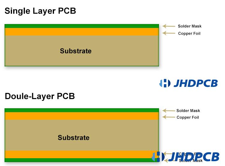
750×552 single double layer pcb jhdpcb
1024×427 comprension de los pcb de doble una guia completa
750×552 single double layer pcb jhdpcb
 760×400 layer pcb layer pcb
 1048×772 design pcb layout circuit basics
 1024×576 double sided pcb types pcb electronics
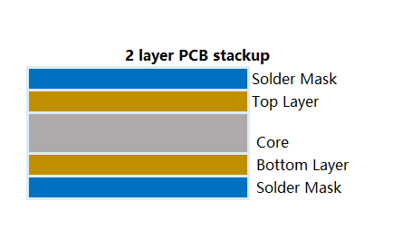
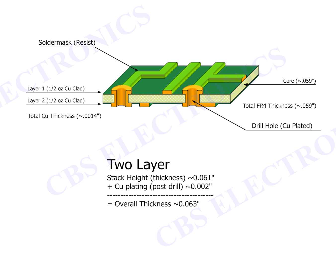 1352×1024 pcb stackups cbs pcb
 1225×641 build multilayer pcb stack sierra circuits
 1000×750 introduction layer pcb
 500×367 layer pcb allpcb allpcbcom
 1200×628 ground planes layer pcb pcb design blog altium
 530×310 layer layer pcbhow choose pcba tech
 1280×720 eevblog pcb emc pcb
 500×400 whats difference single double sided printed circuit
 1420×535 pcb stack guide examples san francisco circuits
 2000×1333 supply layer enig pcb wholesale factory multech pcb technologies
 1280×720 difference layer pcb layer pcb
 474×313 introduction double sided pcb engineering projects
 1280×720 printed circuit boards single double multi layer
 342×285 construction double sided pcb engineering knowledge
 1920×1040 pcb pcm salary pcb pcba
 434×254 layer pcbs double sided pcb boards circuit board design
 1400×875 pcbway layer stack aksesoris pcbway layer stackup skema pcb
 530×310 choose layer pcb layer pcb
 770×263 tknolozh pcb
 500×333 standard multi layer pcb stack ups layers
 534×275 esquemas disenos de pcb
 1000×611 introduction layer pcb raypcb
 520×520 layers pcb board standard pcbquickturn pcbbonding pcb
 1000×750 double layer pcb complete guide ibe
 600×282 layer pcb singapore quality double layer pcb fabrication
 1000×478 layer layer pcb project pcba
 785×657 layer pcb design singapore electronic circuit
 536×410 plan multilayer pcb stackup raypcb
Don’t forget to bookmark Two Layer Pcb by pressing Ctrl + D (PC) or Command + D (macOS). If you are using a mobile phone, you can also use the browser’s drawer menu. Whether it's Windows, Mac, iOS, or Android, you can download images using the download button.