
If you are looking for Package Substrate, you are in the right place. We have 26 images of Package Substrate, including pictures, photos, wallpapers, and more. On this page, we also have a variety of images available, such as png, jpg, animated gifs, artwork, logos, black and white, transparent, and more.
Not only Package Substrate, but you can also find other images such as What Is BOC, Intel CPU, Buckle Delamination, Texas Instruments, High Density, IC, Glass, Silicon, Baked, Bump For, Lpddr5 Mounted, Heated, Dual In-Line Package, Ball Grid Array, Chip Carrier, Pin Grid Array, Electronic Packaging, Surface-mount Technology, Flip Chip, Wire Bonding, Land Grid Array, and Wafer.
 4608×2096 sip package substrate bt material layer enepig
 2855×887 dnp develops tgv glass core substrate semiconductor packages dnp
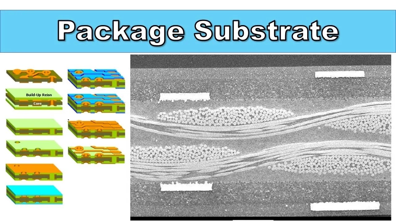 1280×720 package substrate comprehensive exploration ibe electronics
 1000×750 top global package substrate suppliers pcba manufacturers
 911×377 polymers electronic packaging introduction semiconductor
 1140×340 package substrate samsung electro mechanics
 354×250 package substrate kyocera korea
 1000×750 difference package substrate pcb ibe
 1500×701 mdar mjtmaa aa anoaaa aan
 1132×517 analogie pedal kapitane brie solder polyester substrate editor
 600×600 bt fr ic package substrate printed circuit board pcb
 623×254 bga package types
 1280×1047 scc chip package substrate
 1000×567 types chip packaging substrates ibe electronics
 1143×429 pcb package substrate layer definition electrical
 547×260 main materials ic packaging substrates
 587×534 embedded package substratemodulezhuhai access semiconductor
 500×362 panasonic commercializes substrate material semiconductor
 757×558 tsvrdl passive interposer substrate scientific diagram
640×316 defect challenges grow ic packaging
757×558 tsvrdl passive interposer substrate scientific diagram
640×316 defect challenges grow ic packaging
 1364×364 package substrate improve product reliability venture
 1080×484 revolutionizing electronics system package technology
 1920×1080 intel vigotovlyatime maybutni protsesori na sklyaniy pidkladtsi
 1920×800 pcb pcb design altium
Don’t forget to bookmark Package Substrate by pressing Ctrl + D (PC) or Command + D (macOS). If you are using a mobile phone, you can also use the browser’s drawer menu. Whether it's Windows, Mac, iOS, or Android, you can download images using the download button.