
If you are looking for Diode Reverse Bias, you are in the right place. We have 33 images of Diode Reverse Bias, including pictures, photos, wallpapers, and more. On this page, we also have a variety of images available, such as png, jpg, animated gifs, artwork, logos, black and white, transparent, and more.
Not only Diode Reverse Bias, but you can also find other images such as Leakage Current, Current Equation, Open Switch, Resistor Circuit, Energy Diagram, Pn-Junction, Forward, Diagram, IV, Switch, For Relay Protection, and Hotspot.
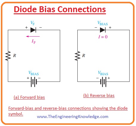
 397×384 diode bias
 346×177 signal diode switching diode characteristics
 622×503 diode characteristic curve
 750×338 pn junction diode reverse bias circuit diagram elle vrogueco
 364×271 diode connected biased
1431×935 solved applying voltage reverse biased diode solveforum
364×271 diode connected biased
1431×935 solved applying voltage reverse biased diode solveforum
 665×238 test diodes multimeter instrumentation tools
 862×793 reverse bias diode explained characteristic curves
 694×513 diode action
 494×259 electronics pn jnction diode reverse bias
 750×338 semiconductor diode bias reverse bias byjus
 0 x 0
0 x 0
 709×414 reverse bias circuit diagram
 531×595 diode
 1024×538 zener diode works reverse bias
 2560×1440 zener diode reverse bias
 600×350 whats reverse bias pn junction diodes mad pcb assembly house
 800×450 pn junction diode reverse bias characteristics
 780×458 explicacion precisa del mecanismo de polarizacion inversa del diodo
 568×354 characteristics bias reverse bias
 500×300 pn junction diode vi characteristics
 664×432 semiconductor pn junction diode working p diode vi characteristics
 1000×1000 circuit diagram varactor diode ami martin blog
 840×1160 diode reverse bias
 800×545 reverse biased pn diode engineering projects
 457×424 diode models engineering knowledge
 242×205 electrical discharge pn junction capacitance valuable
 750×470 junction diode characteristics
 735×449 zener diode principle working usage
 344×296 bias reverse bias applications etechnog
Don’t forget to bookmark Diode Reverse Bias by pressing Ctrl + D (PC) or Command + D (macOS). If you are using a mobile phone, you can also use the browser’s drawer menu. Whether it's Windows, Mac, iOS, or Android, you can download images using the download button.